When producing printed circuit boards (PCBs), the first thing you need to do is source and collect the relevant elements. Once you have all of these, the assembly process can begin and these can be mounted to the board itself.
However, there are several ways this can be done and you need to determine which method is going to be best for your project.
The two most common options are surface mount technology (SMT) and through-hole technology (THT). In this guide, we’re going to focus on SMT, looking at how printed circuit boards are assembled in this way and the benefits of using this method.
Read on to find out more.
What is surface mount technology (SMT)?
Contents
Before we begin looking at the process, let’s quickly take a look at the history of SMT and what it actually means.
This technique was developed in the 1960s by IBM and was originally called Planar Mounting. It was initially used for building small-scale computers. However, the technique didn’t really take off until the 1990s when surface-mounted devices became far more popular and widely used.
The term surface mount technology (SMT) refers to the assembly and production method used when applying electronic components directly onto the surface of a PCB. Unlike more traditional assembly methods, SMT components are soldered directly onto the board, rather than having to be inserted through holes to be attached.
This approach can be far more beneficial to businesses as it allows for more of the assembly to be completed by automated production tools over human intervention. This is why it became the preferred method back in the 90s, cutting out tedious and time-consuming manual processes and helping to save businesses a lot of money.
The SMT assembly process
Now we have a deeper understanding of SMT and where it came from, we can dive into the actual assembly process. This will help to develop our knowledge of this type of manufacturing process. The process is broken down into the following five stages:
1. Preparing the PCB and other components
In the first part of the process, the printed circuit board must be designed and the surface mount components (SMCs) selected. The board will be created with flat solder pads rather than holes, these are typically made from silver, tin-lead or gold-plated copper. These pads are made to support the pins of the components.
At this stage, a stencil is also used to provide a fixed position for the next part of the process. All of these materials must be properly examined for flaws before moving on to the next phase.
2. Solder paste printing
Solder paste is a mixture of powdered metal solder and flux that creates a sticky, almost putty-like substance. During this second phase, this solder paste is applied using the aforementioned stencil, usually at an angle of around 45℃ to 60℃.
The flux is used like a temporary glue to hold SMCs in place, as well as cleanse the surfaces of any impurities. The solder paste helps to connect the surface mount components and solder pads to the PCB.
Getting the exact quantity of this paste right is crucial. If this is incorrect, no connection will be established when the solder is melted in the reflow oven, a heating device used in SMT. We’ll talk about this in more detail later on.
3. The components are placed on the PCB
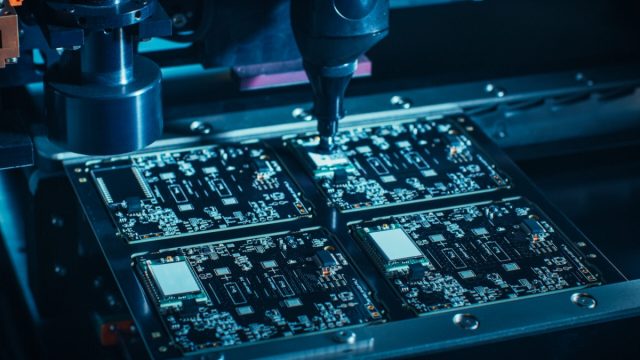
The next tool used in the process is the pick-and-place machine. As each component is removed from its packaging, it is then placed by the machine in the correct location. The PCB will then pass along a conveyor belt as each component is added by quick but extremely accurate tools.
This accuracy is absolutely crucial to ensure that all components are placed and soldered into the right position. Any mistakes can be time-consuming and costly.
4. The PCB enters the reflow oven
After all the components are in the correct position, the PCB is taken to the aforementioned reflow oven. In the oven it will go through several stages, these include:
- The preheat stage: This is where the temperature is raised simultaneously and gradually. It will be raised until it reaches between 140℃ to 160℃
- The soak stage: At this point, the board is held at that temperature for between a minute to a minute and half
- The reflow stage: Next, the temperature is ramped up again to reach between 210℃ and 230℃. This will melt the solder paste and weld each component to the pads on the PCB
- The cooling stage: In this final step, the solder is given the chance to harden and freeze properly before leaving the oven. This helps to avoid joint defects
In some cases, if the PCB is double-sided then this process may be repeated.
5. Cleaning and final inspection
Finally, once the soldering stage is complete, the PCB must be cleaned and carefully inspected to ensure there are no flaws. For the most accurate results, magnifying lenses, automated optical inspection (AOI), flying probe testers and X-ray inspection tools are used.
If any defects around found, these are repaired before the product is stored.


