


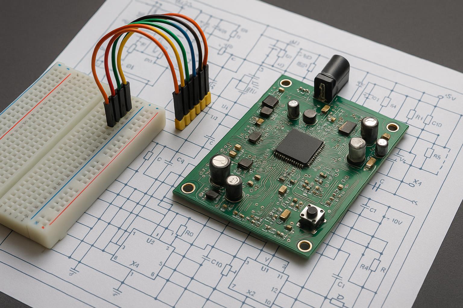
From schematic to physical sample: how a Proto PCB run exposes what simulation software never catches
In electronics development, simulation software can confirm that a circuit’s logic is correct, but few experienced engineers treat a simulation result as the final answer. What actually determines whether a product works reliably is usually whatever the prototype stage exposes.
The importance of prototype validation in hardware development has only grown over the years. Simulation tools catch most of the low-level logic errors in a circuit, but physical-layer problems — electromagnetic interference, thermal distribution, how a material actually performs — still only surface through real-world testing. One board with a wireless module simulated perfectly, but the finished Proto PCB, once powered on, couldn’t reach even half its expected communication range. The root cause turned out to be a carelessly drawn ground plane around the antenna that distorted the radiation pattern — exactly the kind of problem a simulation model will never flag.
Teams also tend to pick a prototyping strategy suited to whatever they’re validating at a given stage. Early in a project, a board might only need to validate core logic, with just the test points required for that. Mid-project, a version closer to the finished product is needed, factoring in enclosure structure and thermal behavior. Only at the end comes the version that’s genuinely ready for volume production. Each stage has a clear goal: get progressively closer to real-world use conditions.
Hardware teams that take prototype validation seriously tend to avoid major rework once volume production starts. Once a problem surfaces after production has already begun, fixing it is rarely as simple as running another prototype — it can mean re-ordering stencils, adjusting the pick-and-place program, or halting the entire production line.
Here are several key methods hardware teams use during Proto PCB runs to test design assumptions and surface potential problems early:
Staged Prototype Validation
Contents
Splitting prototype development into clearly defined stages is the most direct way to control risk. It might start as a bare-bones functional board confirming the core logic works, followed by a version closer to the finished product that accounts for enclosure structure and thermal behavior, and finally a version ready for volume production. Each stage validates something different, and catching a problem at any given stage is always cheaper than catching it after production has started.
Modular design also lowers risk. On one motor driver board project, the power section and control section were built as separable, pluggable modules and tested independently — so if one part had a problem, only that small section needed to be redesigned, rather than starting over from scratch. This step-by-step validation takes more time up front, but debugging afterward goes noticeably faster. Reserving a few extra test pads near key signal lines is a similar habit worth building into the prototype stage — it looks like wasted space, but it saves a lot of trouble with jumper wires during later debugging.
Syncing Process Details With the Manufacturer
If the prototype stage relies purely on design software in isolation, a lot of process-level assumptions never get validated — they only surface once production has already begun, and rework costs go up sharply. Bringing an early design to the factory floor in person, and having an engineer walk through the stack-up structure to explain how different copper thicknesses affect heat dissipation, delivers information that’s usually far more direct than anything exchanged over email.
The first time a 4-layer board was sent out, the fab engineer called proactively to ask whether the inner-layer copper thickness should be increased, since the power traces were too thin for the current they had to carry. That kind of feedback is a sign that a genuinely professional multilayer pcb manufacturer isn’t just executing a file — they’re using their own experience to patch gaps in the design. A similar situation came up with via sizing: a manufacturing partner proactively suggested adjusting via diameter by 0.1mm to improve yield, a level of detail design software itself would never flag.
Validating Key Parameters With Real Measured Data
Some electrical performance issues can only be pinned down with real measured data. Differential signal pairs are a good example: even when trace width and spacing fall within tolerance, a length mismatch of more than 5% between the two lines causes timing skew — a problem that usually needs a TDR tester combined with actual waveform analysis to catch, since automated optical inspection alone isn’t enough.
Vias need the same real-data scrutiny at high frequency. At mmWave frequencies, an unoptimized via can produce more than 0.5dB of insertion loss, which is a serious problem for an RF system — the fix is adding a ring of grounding vias around it and using back-drilling to eliminate the stub effect. Impedance control isn’t a case of applying a textbook number and calling it done, either: the common 50-ohm target isn’t always optimal for high-speed digital circuits — in some cases, dropping to 40 ohms actually improves signal quality, depending on the driving chip’s output strength and the receiver’s sensitivity, which means it has to be tuned dynamically rather than defaulted to a standard value. Plating is another detail that’s easy to underrate but directly determines board lifespan: comparing samples from two factories using the identical design file, one factory’s boards started oxidizing within six months, while the other’s were still working fine after three years. The difference came down to current density control and solution purity during plating.
Choosing Materials and Processes to Fit the Application
Many of the details that matter most at the prototype stage aren’t about the circuit design itself — they’re about whether the material and process choices actually fit the real application. Copper weight on the power layer is a good example: in high-current applications, 1oz copper foil might only handle 2-3A, while 2oz copper foil can comfortably handle 5A or more, a difference that becomes especially clear over long-term operation. It’s worth using heavier copper on the power section even at some extra cost.
Soldermask color deserves a second look, too: black looks more premium, but it’s easier to miss defects when inspecting traces. Different soldermask ink colors also reflect UV light differently — green gives the best visual contrast, while darker soldermask, however good it looks, tends to mask subtle defects like copper corrosion or solder splash. Surface finish selection should stay practical: for consumer electronics with a lifespan under three years stored in dry conditions, OSP can cost roughly a third of ENIG while fully meeting performance needs — but for applications with frequent connector insertion or high-humidity environments, gold-finger plating thickness needs to be tightly controlled. Material choice should also match signal requirements — one high-frequency circuit built on standard FR-4 suffered such severe signal loss it simply didn’t work, and switching to a specialty substrate fixed it; sometimes spending more on the base material up front is the better trade. A space-constrained wearable device might need an experienced multilayer pcb manufacturer capable of holding 0.1mm trace width and spacing reliably on an 8-layer board, while an industrial control board should prioritize noise immunity instead — that kind of application-specific difference is exactly why process choices need to stay flexible rather than defaulting to one standard.
Conclusion
As hardware product cycles keep accelerating, teams that treat every prototype stage as a genuine validation opportunity — rather than just a step to check off — tend to catch most of their potential problems before volume production ever starts. That disciplined move from design assumption to physical validation is the real value of a Proto PCB run, and it’s what separates a hardware engineer from someone doing purely theoretical design.